The Essential Role of FFKM Elastomers in Semiconductor Applications

Elements of this image furnished by Adobe Stock | jeffery
By Austin Walker, Vice President of Sales and Marketing, anyseals, Inc.
Elastomer materials in O-Rings and seals are used in critical, heavily regulated industries including semiconductor chip manufacturing. They must adapt to the increasingly aggressive requirements of their operating environments. How do they achieve this?
It’s simple. This can be achieved using perfluoroelastomers such as FFKM 1418 standard, by the American Society for Testing and Materials (ASTM). FFKM is a type of chemical and heat-resistant elastomers that combine the chemical resistance of polytetrafluoroethylene (PTFE) with the flexibility and elasticity of standard fluorocarbon elastomers (FKM).
Due to their unique properties, FFKM elastomers are widely used in various industrial processes, such as semiconductor manufacturing. To grasp the effectiveness of FFKM, it’s essential to comprehend both its history and how it differs in performance from FKM.
FFKM vs. FKM
FKM, an abbreviation for “Fluorine Kautschuk Material,” was first developed in the late 1950s to meet the aerospace industry’s need for high-performance seals. Since its creation, it has undergone continuous enhancements to improve thermal stability and resistance to heat, solvents, and compression.
FFKM, on the other hand, was initially created in the late 1960s. Full-scale production did not commence until the late 1980s due to patent restrictions. FFKM is utilized in O-rings and seals that must withstand high temperatures or aggressive chemicals. This is valuable in the aerospace, semiconductor, energy, pharmaceutical, and industrial fields.
Despite compelling arguments for using both FFKM and FKM, there are distinct differences between the two when considering their application in highly critical scenarios such as:
- Fluorine Content: FFKM has a higher fluorine content than FKM, which gives it greater resistance to chemicals and high temperatures.
- Temperature Rating: FFKM has a higher temperature rating than FKM, with some FFKM materials able to withstand temperatures up to 325°C/617°F.
- Chemical Compatibility: FFKM is nearly universal in its compatibility with chemicals. It offers outstanding resistance to aggressive acids, organic and inorganic fluids, ketones, esters, solvents, amines, hot water, and steam.
- Electrical Current Resistance and Short-Term Resilience: FFKM has a slight advantage over FKM
Due to its complex chemical composition and manufacturing process, FFKM is known as one of the most expensive elastomer materials. However, it is considered the best option for use in highly demanding applications across various industries. This is true especially those involving high-temperature requirements and strong chemical resistance with almost universal chemical compatibility. The unique needs of semiconductor manufacturers compel the industry to take a closer look at why and where FFKM should be considered for use.
Key Features of FFKM Elastomers
Compared to standard Fluorocarbon Elastomers (FKM), perfluoroelastomers (FFKM) are engineered to provide:
- More stability at high temperatures up to 325 C (617 F).
- Wider operating temperature ranges between -46 to 330 C (-50.8 to 626 F).
- Exceptional chemical resistance and behavior with vacuum applications.
- More effective sealing.
- Increased flexibility in the application.
The Application of FFKM in the Semiconductor Industry
According to a recent report by the IMARC Group1, the global semiconductor market is projected to reach over US $1.1B by 2032. The growing demand for FFKM in semiconductor manufacturing is propelling market expansion.
IMARC also states that the semiconductor industry is undergoing continuous development, with technological advancements leading to increasingly intricate and precise manufacturing processes. Semiconductor devices are becoming more sophisticated, necessitating materials capable of withstanding extreme conditions. FFKMs are renowned for their exceptional resistance to high temperatures, aggressive chemicals, and plasma. This makes them well-suited for use in semiconductor fabrication.
The increasing miniaturization of electronics is generating demand for high-performance materials. FFKM usage is rising with the semiconductor industry expanding to keep up with the growing need for electronic devices. This trend is prominent in regions with robust electronics manufacturing sectors. The advancement of semiconductor technologies, such as advanced lithography and etching, is driving the need for materials that can withstand challenging operational environments, leading to increased demand for FFKMs.
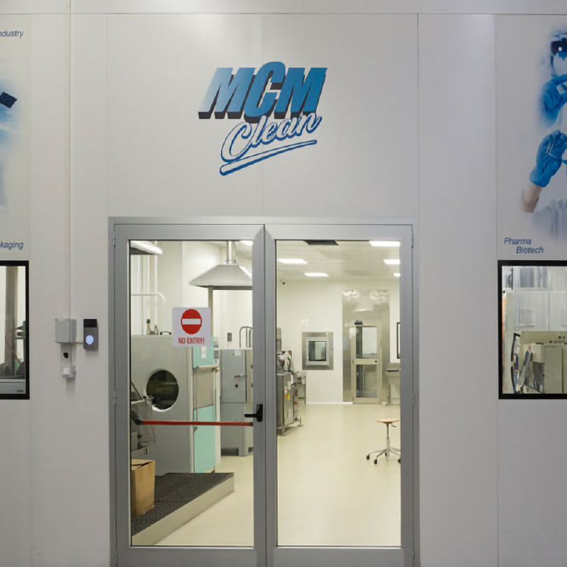
Figure 1 – MCM’s Cleanroom ensures the highest quality standards for precision FFKM manufacturing.
Where to find FFKM O-rings in the semiconductor industry
There are several areas where FFKM O-rings are being used in the semiconductor industry. Examples include:
- Chemical Vapor Deposition (CVD)2 – a process that uses a chemical reaction to create thin films on a heated surface. It’s a vacuum deposition method that’s commonly used in the semiconductor industry to produce high-quality solid materials.
- Chemical Mechanical Polishing (CMP)3 – a process that removes materials using a combination of chemical and mechanical (or abrasive) actions to achieve highly smooth and planar material surfaces.
- Cleaning
- Wet4 – the most common method for cleaning silicon wafers, this uses chemical solutions, deionized water, and sometimes ultrasonic waves, heating, or vacuum techniques. Wet cleaning is damage-free and can remove particles, oxides, metals, and other contaminants.
- Dry5 – uses lasers, aerosols, or ozonated chemistries to clean metalized surfaces. Dry cleaning methods are more selective for various thin films but are limited in the range of contaminants they can address.
- Etching
- Wet6 – uses liquid chemicals or etchants to remove materials from the wafer, usually in specific patterns defined by photoresist masks on the wafer.
- Dry7 – uses ions, usually from a plasma of reactive gases, to dislodge material from the exposed surface of a wafer. The process involves masking out areas of the wafer and then using a masking substance to protect parts of the wafer during multiple etching stages.
- Resist Stripping
- Wet8 – uses solvents to remove photoresists from semiconductor wafers.
- Dry9 – uses plasma or gas-phase chemicals to remove the photoresist from wafers.
- Lithography10 – a series of modules that automatically process wafers to coat or develop them before or after exposure.
- Thermal (LPCVD) nitride11 – a process in which thin films of a semiconductor material are deposited on both sides of the wafer.
- Plasma and gas deposition12 – a technique used to deposit thin films onto a substrate by utilizing plasma to activate chemical reactions within a gas mixture, allowing for deposition at lower temperatures compared to traditional chemical vapor deposition (CVD) methods. Essentially, the plasma energizes the gas molecules, enabling them to readily react and form a film on the surface.
- Photolithography13 – a process using light to transfer a pattern onto a substrate, such as a silicon wafer.
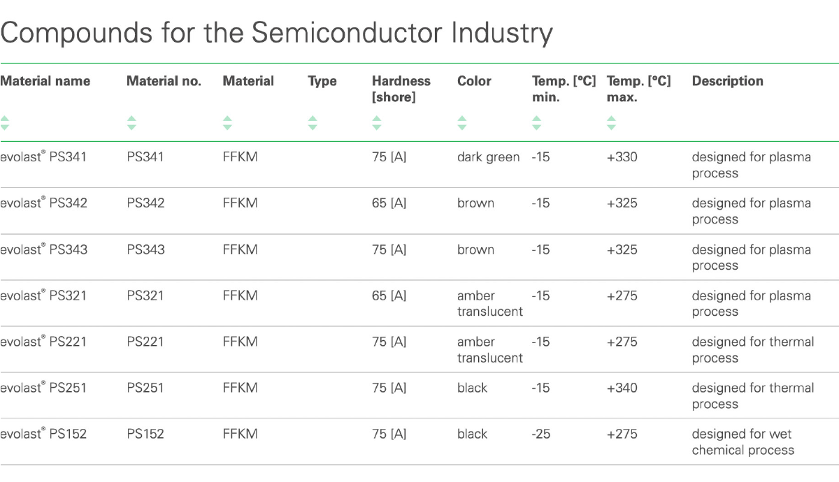
Figure 2 – anyseals, Inc.’s stocks O-rings in a broad range of FFKM compounds. anyseals, Inc.’s stocks O-rings in a broad range of FFKM compounds.
Ultraclean FFKM processing ensures quality
As chipmakers pack in smaller-sized transistors in larger quantities within their chips, they are turning to more demanding manufacturing processes that rely on ultraclean processing. They need seal materials with excellent chemical stability and high heat tolerance. The chemical properties of FFKM make it ideal for many demanding sealing applications in semiconductor fabrication.
In semiconductor manufacturing, it’s critical to maintain a pristine environment. FFKM seals and components are unmatched in their ability to sustain cleanroom standards. Their exceptional chemical resistance and capability to withstand extreme temperatures make FFKM products integral in preventing particulate and chemical contamination, thereby preserving the integrity of the sensitive manufacturing process.
A sister company of anyseals, Inc., MCM is a manufacturer of high-performance, ultra-pure sealing products for the semiconductor industry. MCM understands the importance of meeting the semiconductor industry’s rigorous standards. The company’s state-of-the-art ISO 7 Clean Room production ensures a controlled environment. This helps minimize contaminants and ensures the delivery of high-quality products. Strict cleanliness standards guarantee the integrity of sensitive components and materials during the ISO 7 manufacturing process and ISO 6 sanitizing and packaging process.
In semiconductor manufacturing, contamination poses a significant problem. Even a speck of dust can damage a chip. Components made of FFKM have strong resistance to harsh chemicals and low outgassing, thus greatly reducing the risk of contamination. Consequently, FFKM plays a crucial role in enhancing yield and product quality in the fabrication process.
The relentless push towards miniaturization and complexity in semiconductor devices means that materials used within fabrication must meet the highest purity standards. FFKM materials are engineered to support advanced semiconductor applications, where high performance and precise production are non-negotiable. As semiconductors become more advanced, the need for materials that can maintain integrity under stringent conditions becomes more evident, and FFKM materials are at the forefront of meeting these high-purity demands.
Conclusion
In summary, the use of FFKM elastomers offers exceptional chemical resistance and high-temperature capabilities, making them well-suited for industries like semiconductor manufacturing. The projected expansion of the global semiconductor market further highlights the significance of FFKM in meeting the evolving demands of the industry.
FFKM features higher fluorine content, superior temperature ratings, and excellent chemical compatibility compared to standard FKM elastomers. These FFKM O-rings are utilized in various semiconductor processes, including chemical vapor deposition (CVD), chemical mechanical polishing (CMP), and cleaning protocols. As semiconductor technologies continue to advance, there is an increasing requirement for robust materials such as FFKM that can withstand demanding operational conditions. Consequently, FFKM elastomers are increasingly adopted in critical semiconductor operations to ensure durability and performance under highly stringent conditions.
1 Singh, Suraj. (2024) Semiconductor Market Report 2024-2032 | Industry Size, Growth and Latest Insights. IMARC Group
2 Science Direct, Retrieved September 4, 2024 from https://www.sciencedirect.com/topics/materials-science/chemical-vapor-deposition
3 Science Direct, Retrieved September 4, 2024 from https://www.sciencedirect.com/topics/engineering/chemical-mechanical-polishing
4 CI Semi, Retrieved September 4, 2024 from https://www.ci-semi.com/Wet-Cleaning
5 Utmel Electronics, Retrieved September 4, 2024 from https://www.utmel.com/blog/categories/semiconductor/semiconductor-cleaning-processes-methods-and-reasons
6 Science Direct, Retrieved September 4, 2024 from https://www.sciencedirect.com/topics/materials-science/wet-etching
7 Science Direct, Retrieved September 4, 2024 from https://www.sciencedirect.com/topics/materials-science/dry-etching
8 Abachy, Retrieved September 4, 2024 from https://abachy.com/catalog/semiconductor-equipment/mask-and-reticle-manufacturing-equipment/photolithography-processing-equipment/resist-stripper
9 Abachy, Retrieved September 4, 2024 from https://abachy.com/catalog/semiconductor-equipment/mask-and-reticle-manufacturing-equipment/photolithography-processing-equipment/resist-stripper
10 Science Direct, Retrieved September 4, 2024 from https://www.sciencedirect.com/topics/materials-science/lithography
11 Semicore, Retrieved September 4, 2024 from https://www.semicore.com/news/118-what-is-plasma-enhanced-chemical-vapor-deposition-pecvd
12 Science Direct, Retrieved September 4, 2024 from https://www.sciencedirect.com/topics/materials-science/plasma-deposition
13 Wikipedia, Retrieved September 4, 2024 from https://en.wikipedia.org/wiki/Photolithography


