What Are the Best Pressure Transducers for Semiconductor Applications?
![]()
By Adam Freyler, VP, Ashcroft, Inc.
The semiconductor industry affects nearly every aspect of our lives today. Your cell phone, computer, television, car, and any other electronic device you use each day all depend on semiconductor intelligence. But for those of you who work in the industry, you know that the semiconductor manufacturing process requires highly specialized equipment and instruments that are exceptionally reliable and can handle corrosive gasses and chemicals with stringent contamination control.
Pressure sensors, including pressure transducers and pressure transmitters, for instance, play a critical role in the creation of semiconductors. These instruments measure pressure to control the flow and distribution of ultrahigh purity (UHP) gases and liquids safely and effectively throughout the production process.
This article will provide insight into the unique challenges and solutions for pressure measurement instrumentation used in semiconductor UHP gas and liquid processes. It will also review the best types of pressure transducers that are designed for these complex processes.
Four Primary Challenges of Semiconductor Manufacturing
The equipment and instruments used in these processes must be manufactured in a certain way. A few important considerations include:
1. Contamination Control
Semiconductor manufacturing is constantly challenged to enhance performance and reduce costs. To successfully achieve these, developers continuously increase the circuitry capacity and density on each silicon wafer. This is accomplished by constantly shrinking the size of the features and patterns on the wafer itself, which is often called minimum feature size and measured in nanometers (nm).
As the reduction of circuit pattern sizes continues, it is crucial to maintain strict contamination control measures throughout the manufacturing process to prevent even the most minute foreign particles from damaging the exposed wafer surfaces.
2. Clean and Smooth Surfaces
Clean and smooth surfaces reduce the area exposed to the process and result in shorter times for systems to reach vacuum pressure and remove potential contamination.
Pressure transducers used in the semiconductor process to measure and control the flow of ultra-high purity gases must be intentionally designed to prevent foreign particles from getting inside their cavities. Further, the portion of the sensor exposed to the UHP gases or liquids must be extremely clean and have ultra-smooth surfaces.
3. High-Quality Material
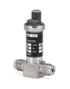
The material used in the construction of pressure instruments needs to be extremely high quality and compatible with the process media. For example, in gas applications, transducers with high-purity grades of 316L stainless steel are commonly recommended due to their high resistance to corrosion as well as their resistance to hydrogen embrittlement. In liquid applications, high-purity grades of fluoropolymers such as polytetrafluoroethylene and perfluoroalkoxy (PTFE/PFA) are commonly used due to their exceptional chemical resistance and prevention of contamination.
4. Safety Approvals for Hazardous Locations
Some of the gases and liquids used in semiconductor applications are toxic, flammable, and otherwise dangerous to those handling them so careful selection of pressure measurement instruments must include appropriate approvals and be made to address critical safety concerns.
These dangers may necessitate approvals for intrinsic safety or non-incendive locations and require approvals such as ATEX and IECEx for these applications.
Intrinsic safety approvals mean the sensor uses a type of barrier that limits the energy applied to an instrument to prevent an explosion from occurring. The barrier is the buffer between the hazardous location and the non-hazardous locations. This is the safest method and is the only method approved for applications where the hazard is continuously present.
Non-incendive safety approvals involve limiting the energy that is applied to an instrument to prevent an explosion without the use of a barrier. The user’s design must limit the energy to the instrument. Non-incendive approvals generally apply to locations where the hazard is not present under normal conditions but has the potential to become hazardous under certain conditions.
Three Factors for Choosing Pressure Transducers for Any Semiconductor Applications
When it comes to the best transducers for the process of semiconductor manufacturing, many of the same features are important for liquid and gas processes. Here are a few other features that are important for gas and liquid applications:
- Repeatability – When purchasing a pressure transducer semiconductor manufacturing, it’s important to trust the measurement your instrument is providing. Ideally, whenever you test the pressure with the same tool, you want a device that will give you a consistent reading every time with no need for zero or span adjustment.
- Durability – Shock, vibration, pressure spikes, and pulsation can all create challenges for semiconductor operations.
If not appropriately designed, pressure transducers can be damaged under harsh operating environments. The best options in this situation are the transducers that are built to withstand rugged conditions. - Accuracy – You’ll also want to confirm the pressure sensor you choose meets the minimum requirements of your specific application. To be sure you have the most accurate measurement, look at the technology the instrument uses for reading pressure.
Some instruments offer a ±0.25% of span accuracy out of the box with zero and span setting errors already included in the specification. This means the unit is ready to be installed with no additional calibration adjustments needed.
The Semiconductor Process
Liquids
The semiconductor manufacturing process is a highly intricate transformation of a blank silicon wafer into discrete microelectronic devices. Generally speaking, the process involves the layering of materials to form pathways and junctions on the wafer that enable the flow and storage of electronic data. During this portion of the manufacturing process, exceptional precision is required to maintain purity and eliminate contamination at the atomic level.
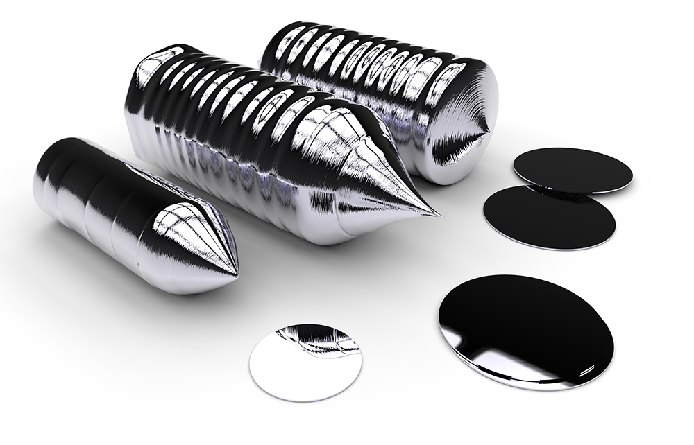
Silicon wafers are large and extremely thin. They are cut with a wire saw from laboratory-grown silicon ingots which are over 99.99% pure. Silicon wafer sizes are commonly 200 – 300mm (7.9 – 11.8 in.) in diameter with a thickness of well under 1mm (0.04 in.). A single wafer is the starting point for the creation of what may be 100’s to 1000’s of individual microelectronic chips.
Two Primary Steps in Liquid Semiconductor Manufacturing
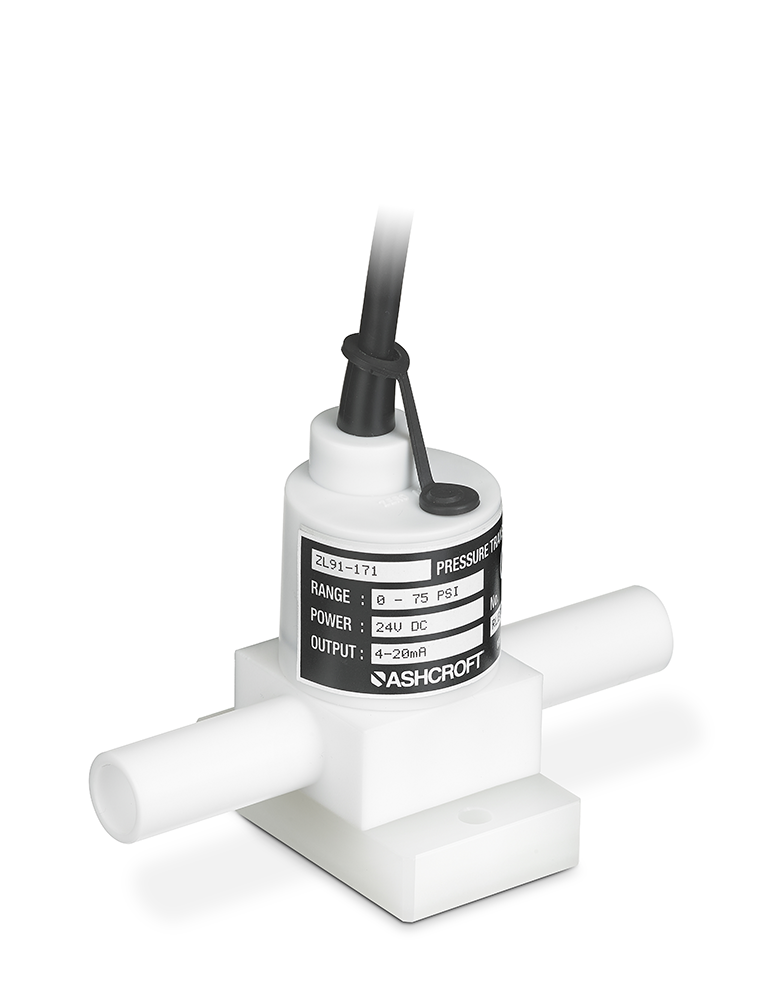
1. Clean and polish the wafer. Wafers must be incredibly flat over their entire surface. To obtain flatness at an atomic level, wafers must be cleaned and polished to a level 1000 times beyond “mirror finish”. One of the prevalent processes used to produce this type of finish is Chemical Mechanical Planarization (CMP). With CMP, a chemical slurry is used to both abrasively and chemically remove any material from the surface of the wafer. Slurries can be alkaline or acidic and include nanoscale particles used for polishing. Removing any impurities, especially metals, is crucial to prevent surface defects on the wafer. To achieve this, any surface that comes in contact with the CMP slurry must be able to withstand abrasion, chemical breakdown, and leaching. In the case of pressure transducers, the design should incorporate high-purity grades of fluoropolymers (such as Teflon™, PTFE, or PFA) as the construction materials.The challenge of using fluoropolymers is that they have relatively poor mechanical properties for a measurement device which requires exceptional precise response to the applied pressure over all process variables. However, a method that combines a PTFE/PFA diaphragm in contact with the fluid that is bonded to a ceramic sensor element, combines the outstanding properties of both materials in this specific application.
2. Wet etching. This step in the semiconductor manufacturing process uses a controlled technique to remove (etch out) select portions of the semiconductor material to define the desired structure or pattern on the blank wafer.
To achieve the desired result, the wet etching process can use extremely powerful alkalis or acids. Some examples of these are Potassium Hydroxide (KOH), Tetramethylammonium hydroxide (TMAH), Hydrochloric Acid (HCL), Hydrofluoric Acid (HF) and Nitric Acid (HNO3). The challenge of handling these liquids includes their ability to leach any impurities contained within the surface of a material as well as penetrating the material itself.
Best features for transducers used in the liquid distribution process of semiconductor manufacturing
- High purity grade PTFE/PFA used for wetted parts for mitigation of both corrosion and minimal contaminant leaching.
- Multiple mounting options for compatibility with different process connections
- A secondary vent design to contain potential gas/vapor permeation
- Digital display (optional)
The Semiconductor Process
Gases
As discussed earlier, semiconductor manufacturing operations also rely on the precise and accurate delivery of ultra-high purity (UHP) gases. UHP gases are required, at times, to exceed purity levels of 99.9995%. Additionally, there may be as many as 49 different UHP gases used1 in the semiconductor production process, often with mixtures being created during a delivery process. After each process step, gases must be completely removed or purged so it does not contaminate a subsequent process step.
Complexities of Gas Semiconductor Manufacturing
Gas delivery systems employed in Semiconductor manufacturing are utilized to manage the important job of injecting these UHP gases.
These systems deliver gases from the source (i.e., a cylinder) to the process chamber where the wafers are located. This delivery generally directs UHP gases at relatively high pressure (compressed) and reduces pressure to near or below atmospheric pressure in the process chamber.
For UHP gas delivery systems to function and control properly, precision measurements are needed to process variables such as pressure, temperature, and flow. In the case of pressure measurements, the pressure transducers used for gas distribution must offer highly accurate and repeatable measurements while maintaining absolute cleanliness inside the system.
Factors that may impact the accuracy of pressure transducers in these applications include the technology used within the device, the materials of construction, and resistance to environmental impacts such as electromagnetic interference (EMI).
Why Materials of Construction Are Vital to the Process
In addition to purity and corrosion resistance, there are a couple of other critical factors to consider when selecting measurement instruments for your semiconductor manufacturing process:
1. Susceptibility to hydrogen exposure. Hydrogen is used in a variety of different semiconductor applications. For instance, it is used as an effective “scavenger gas” to remove oxygen in a crystal growth process called Epitaxy2. But hydrogen also has a unique challenge: it is known to cause embrittlement in certain metals. Embrittlement is a phenomenon that causes loss of ductility and, consequently, brittleness in a material. In a pressure transducer that utilizes a diaphragm to consistently flex like a spring, embrittlement can have a very negative impact on the repeatability and stability of the device. 316L Stainless steel is commonly employed due to its combination of broad resistance to corrosion as well as its strong resistance to hydrogen embrittlement.
2. Electromagnetic Interference (EMI). EMI is the unwanted electromagnetic emissions or disturbances that interfere with the functioning of electronic devices or systems. These interferences can be generated from typical equipment sources found in industrial environments such as from motors and drives. EMI can also be generated from the many unique high voltage/high power processes that may release large amounts of static discharge or create large electromagnetic fields.
EMI can create several undesired effects with instruments like pressure transducers that can impact the accuracy of a signal temporarily, cause long-term drift, reduce the lifespan, or even destroy a device altogether. A standard from the SEMI industry association was created (SEMI E176-1017) to manage and mitigate EMI within semiconductor processes, but it is impossible to fully eliminate it. It is, therefore, very important to select products that meet EMC standards and fully test them in the applications.
 Best features for transducers used in the gas distribution process of semiconductor manufacturing
- High purity grade 316L stainless steel materials
- High resistance to electromagnetic interference (EMI)
- Hazardous location approvals such as ATEX or IECEx
- Digital display (optional)
Changes to Semiconductor Processes are Inevitable
With a better understanding of the challenges in semiconductor UHP gas and liquid processes and the pressure measurement solutions designed to meet those challenges, you can be sure of one thing: change is coming. The global semiconductor industry is expected to continue robust growth over the next few years, so semiconductor suppliers face the challenge of improving supply to meet demand. This includes increasing transistor density, improving reliability, and, of course, reducing production and purchasing costs. This is especially true for materials in emerging technologies such as:
- Artificial intelligence (AI)
- Autonomous driving
- The Internet of Things (IoT)
- 5G—i.e., increasing transistor density, improving reliability, and reducing production and purchasing costs.
Stay informed of the latest trends and innovations in this ever-changing industry and the products that best support its stringent requirements.
Visit Ashcroft.com to learn more.
1 NIST Fluid Metrology Group Index of
Semiconductor Processes Gases
2 Epitaxy – Physical Principles and Technical Implementation ISBN 978-3-642-08737-0


